

Base Year Value ()
x.x %
x.x %
CAGR ()
x.x %
x.x %
Forecast Year Value ()
x.x %
x.x %
Historical Data Period
Largest Region
Forecast Period
半導体計測および検査市場:タイプ別(薄膜計測、リードフレーム検査、ウェーハ検査システム、バンプ検査、マスク検査システムなど)、技術別(電子ビームおよび光学、X線、イオンビーム)、組織規模別(中小企業および大企業)および地域別、2023年から2030年までの世界的な傾向と予測
Instant access to hundreds of data points and trends
- Market estimates from 2014-2029
- Competitive analysis, industry segmentation, financial benchmarks
- Incorporates SWOT, Porter's Five Forces and risk management frameworks
- PDF report or online database with Word, Excel and PowerPoint export options
- 100% money back guarantee
市場概要
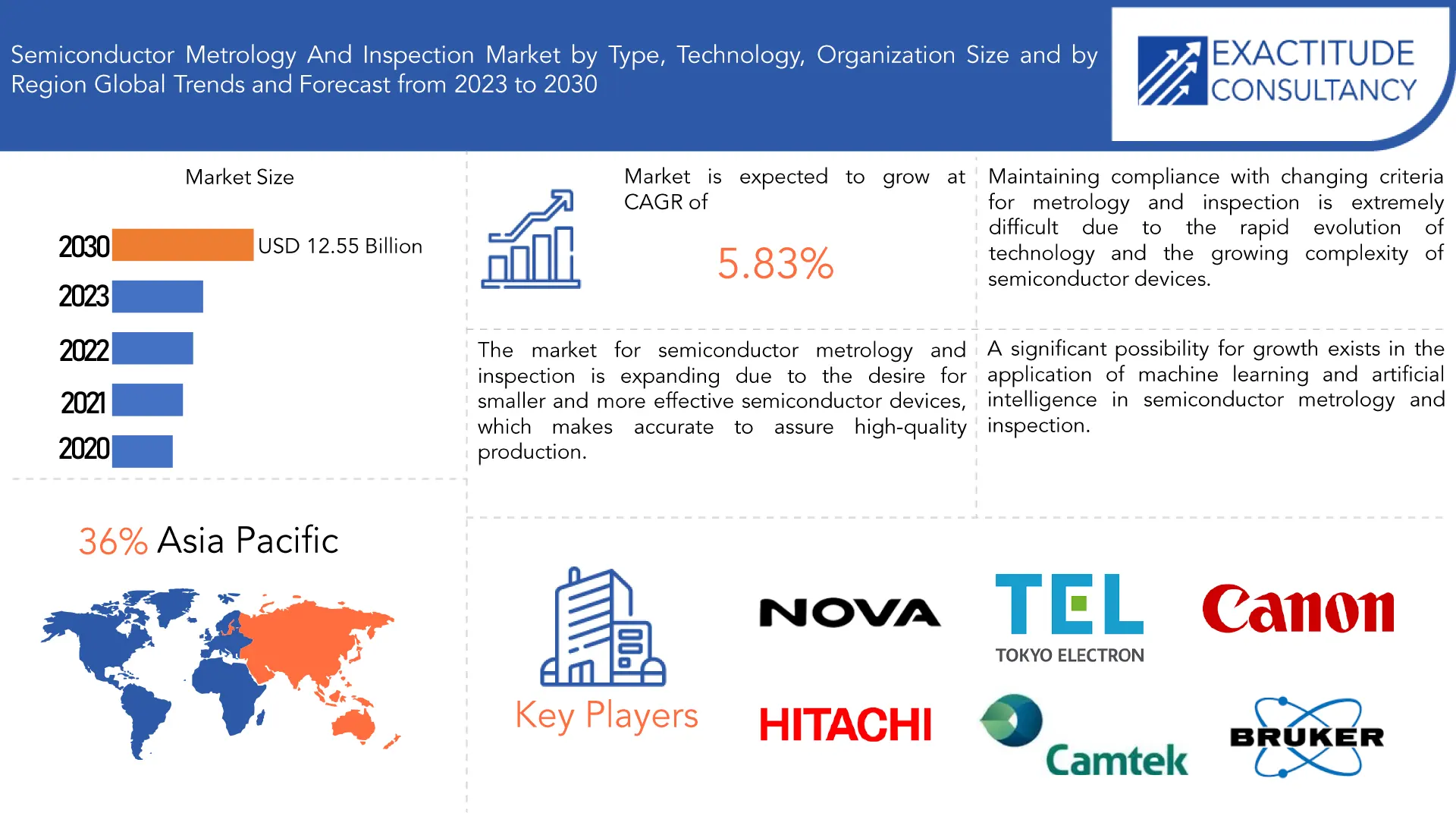
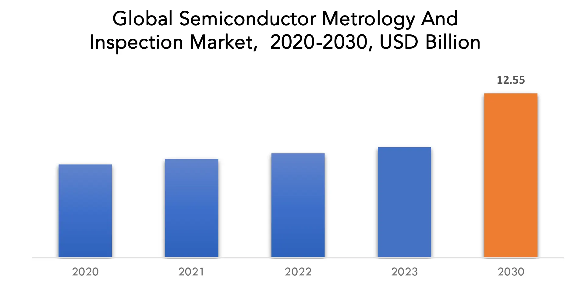
世界の半導体計測および検査市場は、予測期間中に5.83%のCAGRで成長し、2023年の84億4,000万米ドルから2030年には125億5,000万米ドルに達すると予想されています。
さまざまな製造段階での半導体デバイスとコンポーネントの正確な測定と検査は、半導体計測および検査として知られています。設計基準への適合を保証するために、計測には寸法、厚さ、材料組成、電気的特性などの重要な要素の正確な測定が含まれます。検査は、半導体デバイスの機能とパフォーマンスに影響を与える可能性のある欠陥、異常、または汚染物質を見つけることに重点を置いています。これらの手順は、半導体製品の完全性と品質を維持し、歩留まりを向上させ、半導体技術の進化を支援するために不可欠です。最終的に、半導体計測および検査は、高品質で信頼性が高く、効果的な電子デバイスの作成に役立ちます。イオンミル、CV システム、干渉計、ソース メジャー ユニット (SME) 磁力計、光学および画像システム、プロファイロメータ、反射計、抵抗プローブ、抵抗高エネルギー電子回折 (RHEED) システム、X 線回折計は、半導体計測で使用される機器のほんの一部です。統計的プロセス制御により、毎日生産される数千枚のウェーハの代表的なサンプルを検査することで、企業は最小限の作業で生産量と製品品質を向上させることができます。その結果、計測/検査システムの収益の伸びは、機器の伸びよりも緩やかです。多くの企業が、半導体計測/検査機器市場で、開発と革新を示す新製品を発売しています。[caption id="attachment_33542" align="aligncenter" width="1920"]
| 属性 | 詳細 |
| 研究期間 | 2020-2030 |
| 基準年 | 2022 |
| 推定年 | 2023 |
| 予測年 | 2023-2030 |
| 歴史的時代 | 2019-2021 |
| ユニット | 価値(10億米ドル) |
| セグメンテーション | タイプ別、テクノロジー別、組織規模別、地域別 |
| タイプ別 |
|
| テクノロジー別 |
|
| 組織規模別 |
|
| 地域別 |
|
Frequently Asked Questions
• What is the market size for the semiconductor metrology and inspection market?
The global Semiconductor Metrology and Inspection market is anticipated to grow from USD 8.44 Billion in 2023 to USD 12.55 Billion by 2030, at a CAGR of 5.83% during the forecast period.
• Which region is domaining in the semiconductor metrology and inspection market?
Asia Pacific accounted for the largest market in the semiconductor metrology and inspection market. Asia Pacific accounted for 36% market share of the global market value.
• Who are the major key players in the semiconductor metrology and inspection market?
Thermo Fisher Scientific Inc., Onto Innovation, NOVA, Nearfield Instruments B.V., Lasertec Corporation, KLA Corporation, JEOL Ltd., Hitachi, Ltd., Canon U.S.A., Inc., ASML, Applied Materials, Inc., Lasertec CorporatioN, Nikon Metrology NV (Nikon Group), Camtek Limited, Teradyne, Tokyo Electron, Carl Zeiss, Bruker, Rudolph Technologies, Nanometrics
• What is the latest trend in the semiconductor metrology and inspection market?
The creation of fresh metrology and inspection methods for novel semiconductor device types: New semiconductor device kinds, such sensors and actuators, are continually being developed by the semiconductor industry. New metrology and inspection methodologies are necessary for these new devices. Companies that specialize in semiconductor metrology and inspection are creating new methods to check these novel devices for flaws.
Semiconductor Metrology And Inspection Market Segmentation Analysis
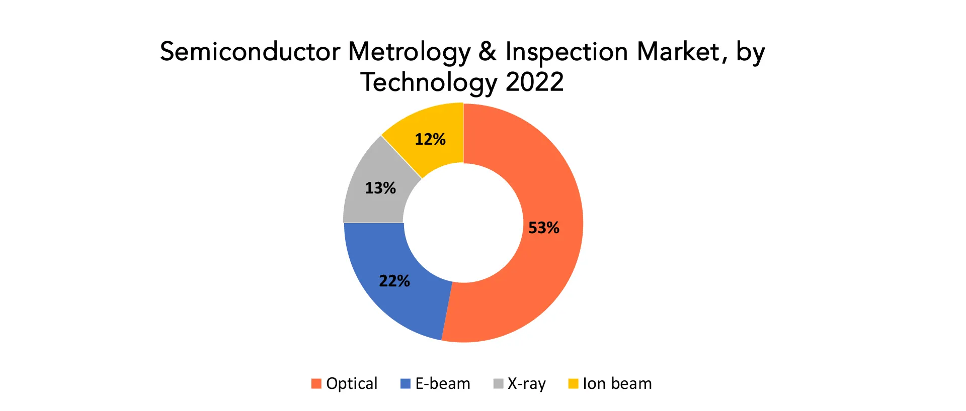
The global semiconductor metrology and inspection market is divided into 4 segments type, technology, organization size and region. Based on type, the semiconductor metrology and inspection market is classified into thin film metrology, lead frame inspection, wafer inspection system, bump inspection, mask inspection system, and others. The market is categorized into e-beam and optical, x-ray, ion beam based on technology. By organization size, the semiconductor metrology and inspection market is divided into small & medium enterprises and large enterprises. [caption id="attachment_33544" align="aligncenter" width="1920"]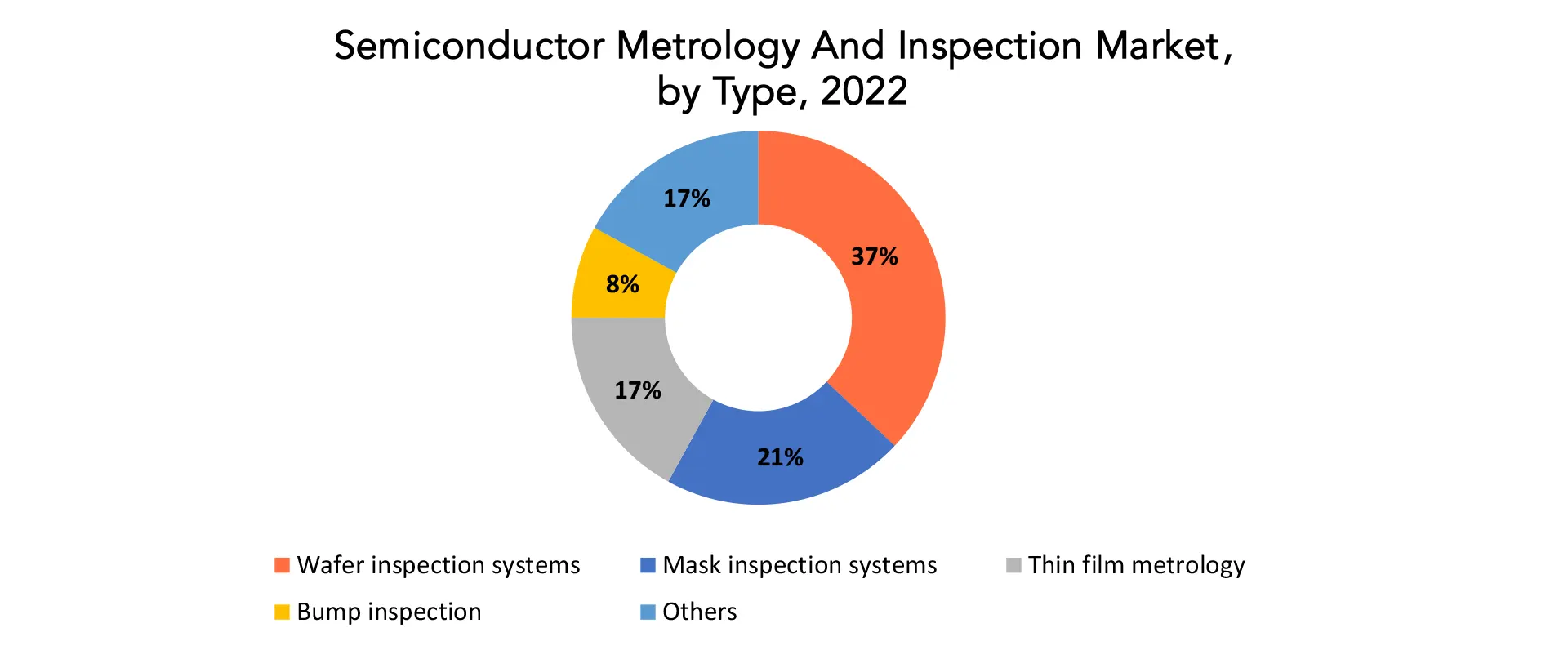
Semiconductor Metrology And Inspection Market Dynamics
Driver The market for cost-effective, high-performance semiconductors is driving growth in the semiconductor metrology and inspection sector. The market for low-cost, exceptionally well semiconductors is driving growth in the semiconductor metrology and inspection sector. The growth of electronics for consumer use, the growing popularity of 5G networks, the launch of IoT devices, and improvements in the field of artificial intelligence (AI) are a few of the causes driving the rise in demand. The need for semiconductors with high performance and low cost is rising as these technologies spread across society. Manufacturers of semiconductors are putting money into cutting-edge metrology and inspection technologies to satisfy these needs. To guarantee that high-quality semiconductors are produced that adhere to exacting standards, accurate measurement and defect detection are essential. The use of metrology and inspection technology is crucial for streamlining production procedures, eliminating faults, raising yield rates, and eventually saving costs. Additionally, as semiconductor components get smaller and more complicated, accurate metrology and defect inspection become more and more crucial. This is particularly true for cutting-edge nodes and technologies like FinFET and 3D stacking, where even the smallest flaws or variations can have a big influence on performance. Restraint The market is hindered by high setup and maintenance costs as well as a lack of expertise in effectively managing metrology systems. The market is hindered by high setup and maintenance costs as well as a lack of expertise in effectively managing metrology systems. The high upfront and ongoing expenditures of putting in place advanced metrology equipment pose challenges for the semiconductor metrology and inspection sector. Advanced metrology tool acquisition, integration with current production processes, and staff training come with a hefty upfront cost. As specialized specialists and ongoing upgrades are required to guarantee optimal system performance and accuracy, high maintenance expenses place additional financial strain on budgets. There aren't many experienced workers with the knowledge to handle and operate this intricate metrology equipment. The gap between technical improvements and the competence needed to manage these advancements expands as technology develops quickly. Smaller businesses and emerging markets seeking to implement sophisticated metrology systems face barriers due to cost and expertise-related issues. It takes coordinated efforts to push for cost-efficiency in system setup and maintenance, as well as steps to improve training programmers and information exchange within the industry, in order to overcome these obstacles and ultimately enable more seamless integration and operation of metrology systems. Opportunities During the projection period, the worldwide market has potential due to the rising demand for semiconductor wafers in consumer electronics. Due to the increased demand for semiconductor wafers in consumer electronics, the global market for semiconductor metrology and inspection is anticipated to expand significantly over the forecasted period. The semiconductor industry is under pressure to provide effective and high-quality parts due to the rise in popularity of consumer electronics including cellphones, tablets, laptops, and other devices. This increase is further spurred by developing markets, where semiconductors are essential components, such 5G, IoT, AI, and electric vehicles. To improve performance and power efficiency, the semiconductor industry is moving towards smaller nodes and cutting-edge packaging methods. For these little semiconductor components to be precise and reliable, metrology and inspection are essential. Meeting the strict quality requirements required by the industry requires precise measurements, fault identification, and process control. Semiconductor producers must make investments in cutting-edge metrology and inspection technologies to improve manufacturing processes and reduce errors as competition heats up and customer demands grow. The consumer electronics sector is likely to continue to see strong growth over the forecasted period, which will drive demand for better semiconductor wafers.Semiconductor Metrology And Inspection Market Trends
- The creation of novel metrology and inspection methods for sophisticated packaging In the semiconductor industry, advanced packaging techniques including fan-out wafer-level packaging (FOWLP) and system-in-package (SiP) are gaining popularity. These packaging solutions provide a multitude of benefits, including improved performance, reduced size, and cheaper cost.
- The application of AI and ML in metrology and inspection is growing: New metrology and inspection methods that are more precise and effective are being developed with the use of AI and ML. For instance, flaw detection and classification in semiconductor devices may be carried out automatically using AI-powered metrology systems. This may aid in cutting down on inspection expenses and time.
- The creation of fresh metrology and inspection methods for novel semiconductor device types: New semiconductor device kinds, such sensors and actuators, are continually being developed by the semiconductor industry. New metrology and inspection methodologies are necessary for these new devices. Companies that specialize in semiconductor metrology and inspection are creating new methods to check these novel devices for flaws.
- The increasing use of machine learning (ML) and artificial intelligence (AI) New metrology and inspection methods that are more precise and effective are being developed with the use of AI and ML.
- The expanding application of cutting-edge packaging technology The packaging of semiconductor devices is becoming smaller and more intricate because to the adoption of advanced packaging methods. The need for metrology and inspection tools that can check these sophisticated packages is being driven by this.
Competitive Landscape
The competitive landscape of the semiconductor metrology and inspection market was dynamic, with several prominent companies competing to provide innovative and advanced semiconductor metrology and inspection solutions.- Thermo Fisher Scientific Inc.
- Onto Innovation
- NOVA
- Nearfield Instruments B.V.
- Lasertec Corporation
- KLA Corporation
- JEOL Ltd.
- Hitachi, Ltd.
- Canon U.S.A., Inc.
- ASML
- Applied Materials, Inc.
- Lasertec CorporatioN
- Nikon Metrology NV (Nikon Group)
- Camtek Limited
- Teradyne
- Tokyo Electron
- Carl Zeiss
- Bruker
- Rudolph Technologies
- Nanometrics
Regional Analysis
Asia Pacific accounted for the largest market in the semiconductor metrology and inspection market. The market for semiconductor metrology and inspection equipment is currently dominated by Asia-Pacific, and it is projected to expand at a CAGR of 5.20% over the next years. Asia-Pacific is one of the important geographical areas for the semiconductor industry in terms of both production and consumption. The Asia-Pacific semiconductors market, which according to SIA is the biggest regional semiconductor market, is dominated by China. Numerous regional businesses are collaborating and entering into cooperative agreements on the market for semiconductor metrology/inspection equipment. Both businesses want to develop an independent, and regulated sector while collaborating more on developing semiconductor packing machinery. [caption id="attachment_33548" align="aligncenter" width="1920"]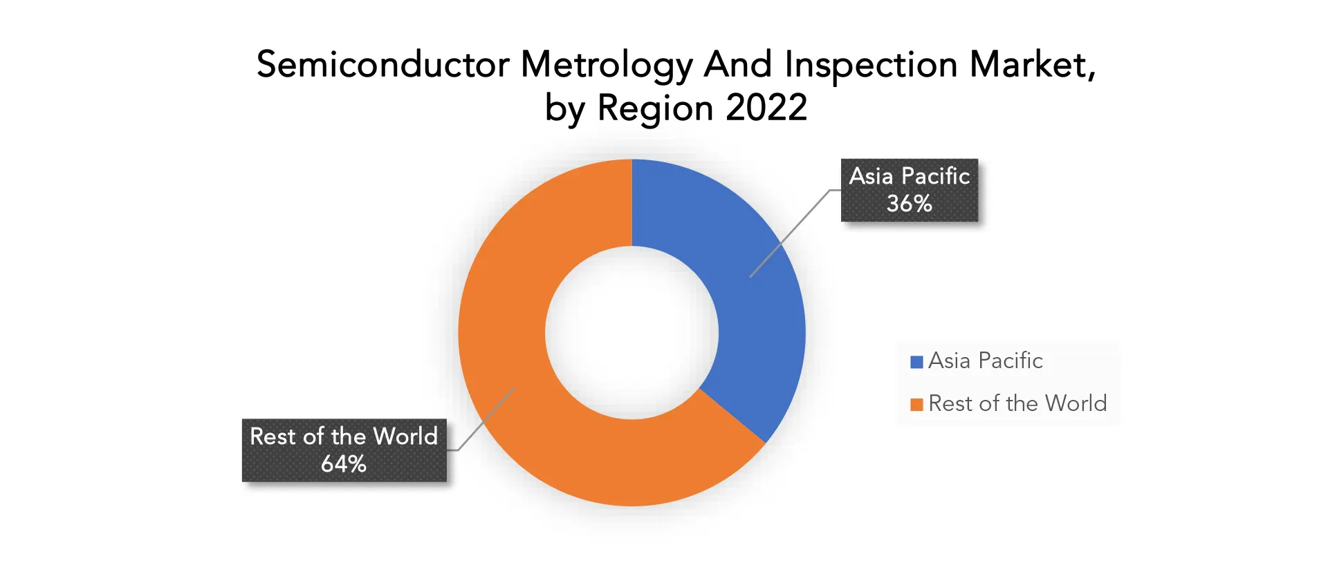
Target Audience for Semiconductor Metrology And Inspection
- Semiconductor Manufacturers
- Semiconductor Equipment Manufacturers
- Research and Development Institutions
- Government and Regulatory Bodies
- Semiconductor Component Suppliers
- Quality Control and Assurance Professionals
- Semiconductor Foundries
- Semiconductor Materials Suppliers
- Industry Associations and Organizations
- Academic Institutions and Universities
Segments Covered in the Semiconductor Metrology And Inspection Market Report
Semiconductor Metrology And Inspection Market by Type- Wafer inspection systems
- Mask inspection systems
- Thin film metrology
- Bump inspection
- Lead frame inspection
- Others
- Optical
- E-beam
- X-ray
- Ion beam
- Large enterprises
- SMEs
- North America
- Europe
- Asia Pacific
- South America
- Middle East and Africa
Key Question Answered
- What is the expected growth rate of the semiconductor metrology and inspection market over the next 7 years?
- Who are the major players in the semiconductor metrology and inspection market and what is their market share?
- What are the end-user industries driving market demand and what is their outlook?
- What are the opportunities for growth in emerging markets such as Asia-pacific, the middle east, and Africa?
- How is the economic environment affecting the semiconductor metrology and inspection market, including factors such as interest rates, inflation, and exchange rates?
- What is the expected impact of government policies and regulations on the semiconductor metrology and inspection market?
- What is the current and forecasted size and growth rate of the global semiconductor metrology and inspection market?
- What are the key drivers of growth in the semiconductor metrology and inspection market?
- Who are the major players in the market and what is their market share?
- What are the distribution channels and supply chain dynamics in the semiconductor metrology and inspection market?
- What are the technological advancements and innovations in the semiconductor metrology and inspection market and their impact on product development and growth?
- What are the regulatory considerations and their impact on the market?
- What are the challenges faced by players in the semiconductor metrology and inspection market and how are they addressing these challenges?
- What are the opportunities for growth and expansion in the semiconductor metrology and inspection market?
- What are the product products and specifications of leading players in the market?
- 導入
- 市場の定義
- 市場セグメンテーション
- 研究タイムライン
- 前提と制限
- 研究方法
- データマイニング
- 二次調査
- 一次研究
- 専門家のアドバイス
- 品質チェック
- 最終レビュー
- データ三角測量
- ボトムアップアプローチ
- トップダウンアプローチ
- 研究の流れ
- データソース
- データマイニング
- エグゼクティブサマリー
- 市場概要
- 半導体計測および検査市場の見通し
- 市場の推進要因
- 市場の制約
- 市場機会
- COVID-19 による半導体計測・検査市場への影響
- ポーターの5つの力モデル
- 新規参入からの脅威
- 代替選手からの脅威
- サプライヤーの交渉力
- 顧客の交渉力
- 競争の度合い
- 業界バリューチェーン分析
- 半導体計測および検査市場の見通し
- 2020年~2030年の世界半導体計測・検査市場(タイプ別)(10億米ドル)
- ウェーハ検査システム
- マスク検査システム
- THIN FILM METROLOGY
- BUMP INSPECTION
- LEAD FRAME INSPECTION
- OTHERS
- GLOBAL SEMICONDUCTOR METROLOGY AND INSPECTION MARKET BY TECHNOLOGY, 2020-2030, (USD BILLION)
- OPTICAL
- E-BEAM
- X-RAY
- ION BEAM
- GLOBAL SEMICONDUCTOR METROLOGY AND INSPECTION MARKET BY ORGANIZATION SIZE, 2020-2030, (USD BILLION)
- LARGE ENTERPRISES
- SMES
- GLOBAL SEMICONDUCTOR METROLOGY AND INSPECTION MARKET BY REGION, 2020-2030, (USD BILLION)
- NORTH AMERICA
- US
- CANADA
- MEXICO
- SOUTH AMERICA
- BRAZIL
- ARGENTINA
- COLOMBIA
- REST OF SOUTH AMERICA
- EUROPE
- GERMANY
- UK
- FRANCE
- ITALY
- SPAIN
- RUSSIA
- REST OF EUROPE
- ASIA PACIFIC
- INDIA
- CHINA
- JAPAN
- SOUTH KOREA
- AUSTRALIA
- SOUTH-EAST ASIA
- REST OF ASIA PACIFIC
- MIDDLE EAST AND AFRICA
- UAE
- SAUDI ARABIA
- SOUTH AFRICA
- REST OF MIDDLE EAST AND AFRICA
- NORTH AMERICA
- COMPANY PROFILES*
(BUSINESS OVERVIEW, COMPANY SNAPSHOT, PRODUCTS OFFERED, RECENT DEVELOPMENTS)
- THERMO FISHER SCIENTIFIC INC.
- ONTO INNOVATION
- NOVA
- NEARFIELD INSTRUMENTS B.V.
- LASERTEC CORPORATION
- KLA CORPORATION
- JEOL LTD.
- HITACHI, LTD
- CANON U.S.A., INC.
- ASML
- APPLIED MATERIALS, INC.
- LASERTEC CORPORATION
- NIKON METROLOGY NV (NIKON GROUP)
- CAMTEK LIMITED
- TERADYNE
- TOKYO ELECTRON
- CARL ZEISS
- BRUKER
- RUDOLPH TECHNOLOGIES
- NANOMETRICS
*THE COMPANY LIST IS INDICATIVE
LIST OF TABLES
TABLE 1 GLOBAL SEMICONDUCTOR METROLOGY AND INSPECTION MARKET BY TYPE (USD BILLION) 2020-2030
TABLE 2 GLOBAL SEMICONDUCTOR METROLOGY AND INSPECTION MARKET BY TECHNOLOGY (USD BILLION) 2020-2030
TABLE 3 GLOBAL SEMICONDUCTOR METROLOGY AND INSPECTION MARKET BY ORGANIZATION SIZE (USD BILLION) 2020-2030
TABLE 4 GLOBAL SEMICONDUCTOR METROLOGY AND INSPECTION MARKET BY REGIONS (USD BILLION) 2020-2030
TABLE 5 NORTH AMERICA SEMICONDUCTOR METROLOGY AND INSPECTION MARKET BY TYPE (USD BILLION) 2020-2030
TABLE 6 NORTH AMERICA SEMICONDUCTOR METROLOGY AND INSPECTION MARKET BY TECHNOLOGY (USD BILLION) 2020-2030
TABLE 7 NORTH AMERICA SEMICONDUCTOR METROLOGY AND INSPECTION MARKET BY ORGANIZATION SIZE (USD BILLION) 2020-2030
TABLE 8 NORTH AMERICA SEMICONDUCTOR METROLOGY AND INSPECTION MARKET BY COUNTRY (USD BILLION) 2020-2030
TABLE 9 US SEMICONDUCTOR METROLOGY AND INSPECTION MARKET BY TYPE (USD BILLION) 2020-2030
TABLE 10 US SEMICONDUCTOR METROLOGY AND INSPECTION MARKET BY TECHNOLOGY (USD BILLION) 2020-2030
TABLE 11 US SEMICONDUCTOR METROLOGY AND INSPECTION MARKET BY ORGANIZATION SIZE (USD BILLION) 2020-2030
TABLE 12 CANADA SEMICONDUCTOR METROLOGY AND INSPECTION MARKET BY TYPE (USD BILLION) 2020-2030
TABLE 13 CANADA SEMICONDUCTOR METROLOGY AND INSPECTION MARKET BY TECHNOLOGY (USD BILLION) 2020-2030
TABLE 14 CANADA SEMICONDUCTOR METROLOGY AND INSPECTION MARKET BY ORGANIZATION SIZE (USD BILLION) 2020-2030
TABLE 15 MEXICO SEMICONDUCTOR METROLOGY AND INSPECTION MARKET BY TYPE (USD BILLION) 2020-2030
TABLE 16 MEXICO SEMICONDUCTOR METROLOGY AND INSPECTION MARKET BY TECHNOLOGY (USD BILLION) 2020-2030
TABLE 17 MEXICO SEMICONDUCTOR METROLOGY AND INSPECTION MARKET BY ORGANIZATION SIZE (USD BILLION) 2020-2030
TABLE 18 SOUTH AMERICA SEMICONDUCTOR METROLOGY AND INSPECTION MARKET BY TYPE (USD BILLION) 2020-2030
TABLE 19 SOUTH AMERICA SEMICONDUCTOR METROLOGY AND INSPECTION MARKET BY TECHNOLOGY (USD BILLION) 2020-2030
TABLE 20 SOUTH AMERICA SEMICONDUCTOR METROLOGY AND INSPECTION MARKET BY ORGANIZATION SIZE (USD BILLION) 2020-2030
TABLE 21 SOUTH AMERICA SEMICONDUCTOR METROLOGY AND INSPECTION MARKET BY COUNTRY (USD BILLION) 2020-2030
TABLE 22 BRAZIL SEMICONDUCTOR METROLOGY AND INSPECTION MARKET BY TYPE (USD BILLION) 2020-2030
TABLE 23 BRAZIL SEMICONDUCTOR METROLOGY AND INSPECTION MARKET BY TECHNOLOGY (USD BILLION) 2020-2030
TABLE 24 BRAZIL SEMICONDUCTOR METROLOGY AND INSPECTION MARKET BY ORGANIZATION SIZE (USD BILLION) 2020-2030
TABLE 25 ARGENTINA SEMICONDUCTOR METROLOGY AND INSPECTION MARKET BY TYPE (USD BILLION) 2020-2030
TABLE 26 ARGENTINA SEMICONDUCTOR METROLOGY AND INSPECTION MARKET BY TECHNOLOGY (USD BILLION) 2020-2030
TABLE 27 ARGENTINA SEMICONDUCTOR METROLOGY AND INSPECTION MARKET BY ORGANIZATION SIZE (USD BILLION) 2020-2030
TABLE 28 COLOMBIA SEMICONDUCTOR METROLOGY AND INSPECTION MARKET BY TYPE (USD BILLION) 2020-2030
TABLE 29 COLOMBIA SEMICONDUCTOR METROLOGY AND INSPECTION MARKET BY TECHNOLOGY (USD BILLION) 2020-2030
TABLE 30 COLOMBIA SEMICONDUCTOR METROLOGY AND INSPECTION MARKET BY ORGANIZATION SIZE (USD BILLION) 2020-2030
TABLE 31 REST OF SOUTH AMERICA SEMICONDUCTOR METROLOGY AND INSPECTION MARKET BY TYPE (USD BILLION) 2020-2030
TABLE 32 REST OF SOUTH AMERICA SEMICONDUCTOR METROLOGY AND INSPECTION MARKET BY TECHNOLOGY (USD BILLION) 2020-2030
TABLE 33 REST OF SOUTH AMERICA SEMICONDUCTOR METROLOGY AND INSPECTION MARKET BY ORGANIZATION SIZE (USD BILLION) 2020-2030
TABLE 34 ASIA-PACIFIC SEMICONDUCTOR METROLOGY AND INSPECTION MARKET BY TYPE (USD BILLION) 2020-2030
TABLE 35 ASIA-PACIFIC SEMICONDUCTOR METROLOGY AND INSPECTION MARKET BY TECHNOLOGY (USD BILLION) 2020-2030
TABLE 36 ASIA-PACIFIC SEMICONDUCTOR METROLOGY AND INSPECTION MARKET BY ORGANIZATION SIZE (USD BILLION) 2020-2030
TABLE 37 ASIA-PACIFIC SEMICONDUCTOR METROLOGY AND INSPECTION MARKET BY COUNTRY (USD BILLION) 2020-2030
TABLE 38 INDIA SEMICONDUCTOR METROLOGY AND INSPECTION MARKET BY TYPE (USD BILLION) 2020-2030
TABLE 39 INDIA SEMICONDUCTOR METROLOGY AND INSPECTION MARKET BY TECHNOLOGY (USD BILLION) 2020-2030
TABLE 40 INDIA SEMICONDUCTOR METROLOGY AND INSPECTION MARKET BY ORGANIZATION SIZE (USD BILLION) 2020-2030
TABLE 41 CHINA SEMICONDUCTOR METROLOGY AND INSPECTION MARKET BY TYPE (USD BILLION) 2020-2030
TABLE 42 CHINA SEMICONDUCTOR METROLOGY AND INSPECTION MARKET BY TECHNOLOGY (USD BILLION) 2020-2030
TABLE 43 CHINA SEMICONDUCTOR METROLOGY AND INSPECTION MARKET BY ORGANIZATION SIZE (USD BILLION) 2020-2030
TABLE 44 JAPAN SEMICONDUCTOR METROLOGY AND INSPECTION MARKET BY TYPE (USD BILLION) 2020-2030
TABLE 45 JAPAN SEMICONDUCTOR METROLOGY AND INSPECTION MARKET BY TECHNOLOGY (USD BILLION) 2020-2030
TABLE 46 JAPAN SEMICONDUCTOR METROLOGY AND INSPECTION MARKET BY ORGANIZATION SIZE (USD BILLION) 2020-2030
TABLE 47 SOUTH KOREA SEMICONDUCTOR METROLOGY AND INSPECTION MARKET BY TYPE (USD BILLION) 2020-2030
TABLE 48 SOUTH KOREA SEMICONDUCTOR METROLOGY AND INSPECTION MARKET BY TECHNOLOGY (USD BILLION) 2020-2030
TABLE 49 SOUTH KOREA SEMICONDUCTOR METROLOGY AND INSPECTION MARKET BY ORGANIZATION SIZE (USD BILLION) 2020-2030
TABLE 50 AUSTRALIA SEMICONDUCTOR METROLOGY AND INSPECTION MARKET BY TYPE (USD BILLION) 2020-2030
TABLE 51 AUSTRALIA SEMICONDUCTOR METROLOGY AND INSPECTION MARKET BY TECHNOLOGY (USD BILLION) 2020-2030
TABLE 52 AUSTRALIA SEMICONDUCTOR METROLOGY AND INSPECTION MARKET BY ORGANIZATION SIZE (USD BILLION) 2020-2030
TABLE 53 SOUTH-EAST ASIA SEMICONDUCTOR METROLOGY AND INSPECTION MARKET BY TYPE (USD BILLION) 2020-2030
TABLE 54 SOUTH-EAST ASIA SEMICONDUCTOR METROLOGY AND INSPECTION MARKET BY TECHNOLOGY (USD BILLION) 2020-2030
TABLE 55 SOUTH-EAST ASIA SEMICONDUCTOR METROLOGY AND INSPECTION MARKET BY ORGANIZATION SIZE (USD BILLION) 2020-2030
TABLE 56 REST OF ASIA PACIFIC SEMICONDUCTOR METROLOGY AND INSPECTION MARKET BY TYPE (USD BILLION) 2020-2030
TABLE 57 REST OF ASIA PACIFIC SEMICONDUCTOR METROLOGY AND INSPECTION MARKET BY TECHNOLOGY (USD BILLION) 2020-2030
TABLE 58 REST OF ASIA PACIFIC SEMICONDUCTOR METROLOGY AND INSPECTION MARKET BY ORGANIZATION SIZE (USD BILLION) 2020-2030
TABLE 59 EUROPE SEMICONDUCTOR METROLOGY AND INSPECTION MARKET BY TYPE (USD BILLION) 2020-2030
TABLE 60 EUROPE SEMICONDUCTOR METROLOGY AND INSPECTION MARKET BY TECHNOLOGY (USD BILLION) 2020-2030
TABLE 61 EUROPE SEMICONDUCTOR METROLOGY AND INSPECTION MARKET BY ORGANIZATION SIZE (USD BILLION) 2020-2030
TABLE 62 EUROPE SEMICONDUCTOR METROLOGY AND INSPECTION MARKET BY COUNTRY (USD BILLION) 2020-2030
TABLE 63 GERMANY SEMICONDUCTOR METROLOGY AND INSPECTION MARKET BY TYPE (USD BILLION) 2020-2030
TABLE 64 GERMANY SEMICONDUCTOR METROLOGY AND INSPECTION MARKET BY TECHNOLOGY (USD BILLION) 2020-2030
TABLE 65 GERMANY SEMICONDUCTOR METROLOGY AND INSPECTION MARKET BY ORGANIZATION SIZE (USD BILLION) 2020-2030
TABLE 66 UK SEMICONDUCTOR METROLOGY AND INSPECTION MARKET BY TYPE (USD BILLION) 2020-2030
TABLE 67 UK SEMICONDUCTOR METROLOGY AND INSPECTION MARKET BY TECHNOLOGY (USD BILLION) 2020-2030
TABLE 68 UK SEMICONDUCTOR METROLOGY AND INSPECTION MARKET BY ORGANIZATION SIZE (USD BILLION) 2020-2030
TABLE 69 FRANCE SEMICONDUCTOR METROLOGY AND INSPECTION MARKET BY TYPE (USD BILLION) 2020-2030
TABLE 70 FRANCE SEMICONDUCTOR METROLOGY AND INSPECTION MARKET BY TECHNOLOGY (USD BILLION) 2020-2030
TABLE 71 FRANCE SEMICONDUCTOR METROLOGY AND INSPECTION MARKET BY ORGANIZATION SIZE (USD BILLION) 2020-2030
TABLE 72 ITALY SEMICONDUCTOR METROLOGY AND INSPECTION MARKET BY TYPE (USD BILLION) 2020-2030
TABLE 73 ITALY SEMICONDUCTOR METROLOGY AND INSPECTION MARKET BY TECHNOLOGY (USD BILLION) 2020-2030
TABLE 74 ITALY SEMICONDUCTOR METROLOGY AND INSPECTION MARKET BY ORGANIZATION SIZE (USD BILLION) 2020-2030
TABLE 75 SPAIN SEMICONDUCTOR METROLOGY AND INSPECTION MARKET BY TYPE (USD BILLION) 2020-2030
TABLE 76 SPAIN SEMICONDUCTOR METROLOGY AND INSPECTION MARKET BY TECHNOLOGY (USD BILLION) 2020-2030
TABLE 77 SPAIN SEMICONDUCTOR METROLOGY AND INSPECTION MARKET BY ORGANIZATION SIZE (USD BILLION) 2020-2030
TABLE 78 RUSSIA SEMICONDUCTOR METROLOGY AND INSPECTION MARKET BY TYPE (USD BILLION) 2020-2030
TABLE 79 RUSSIA SEMICONDUCTOR METROLOGY AND INSPECTION MARKET BY TECHNOLOGY (USD BILLION) 2020-2030
TABLE 80 RUSSIA SEMICONDUCTOR METROLOGY AND INSPECTION MARKET BY ORGANIZATION SIZE (USD BILLION) 2020-2030
TABLE 81 REST OF EUROPE SEMICONDUCTOR METROLOGY AND INSPECTION MARKET BY TYPE (USD BILLION) 2020-2030
TABLE 82 REST OF EUROPE SEMICONDUCTOR METROLOGY AND INSPECTION MARKET BY TECHNOLOGY (USD BILLION) 2020-2030
TABLE 83 REST OF EUROPE SEMICONDUCTOR METROLOGY AND INSPECTION MARKET BY ORGANIZATION SIZE (USD BILLION) 2020-2030
TABLE 84 MIDDLE EAST AND AFRICA SEMICONDUCTOR METROLOGY AND INSPECTION MARKET BY TYPE (USD BILLION) 2020-2030
TABLE 85 MIDDLE EAST AND AFRICA SEMICONDUCTOR METROLOGY AND INSPECTION MARKET BY TECHNOLOGY (USD BILLION) 2020-2030
TABLE 86 MIDDLE EAST AND AFRICA SEMICONDUCTOR METROLOGY AND INSPECTION MARKET BY ORGANIZATION SIZE (USD BILLION) 2020-2030
TABLE 87 MIDDLE EAST AND AFRICA SEMICONDUCTOR METROLOGY AND INSPECTION MARKET BY COUNTRY (USD BILLION) 2020-2030
TABLE 88 UAE SEMICONDUCTOR METROLOGY AND INSPECTION MARKET BY TYPE (USD BILLION) 2020-2030
TABLE 89 UAE SEMICONDUCTOR METROLOGY AND INSPECTION MARKET BY TECHNOLOGY (USD BILLION) 2020-2030
TABLE 90 UAE SEMICONDUCTOR METROLOGY AND INSPECTION MARKET BY ORGANIZATION SIZE (USD BILLION) 2020-2030
TABLE 91 SAUDI ARABIA SEMICONDUCTOR METROLOGY AND INSPECTION MARKET BY TYPE (USD BILLION) 2020-2030
TABLE 92 SAUDI ARABIA SEMICONDUCTOR METROLOGY AND INSPECTION MARKET BY TECHNOLOGY (USD BILLION) 2020-2030
TABLE 93 SAUDI ARABIA SEMICONDUCTOR METROLOGY AND INSPECTION MARKET BY ORGANIZATION SIZE (USD BILLION) 2020-2030
TABLE 94 SOUTH AFRICA SEMICONDUCTOR METROLOGY AND INSPECTION MARKET BY TYPE (USD BILLION) 2020-2030
TABLE 95 SOUTH AFRICA SEMICONDUCTOR METROLOGY AND INSPECTION MARKET BY TECHNOLOGY (USD BILLION) 2020-2030
TABLE 96 SOUTH AFRICA SEMICONDUCTOR METROLOGY AND INSPECTION MARKET BY ORGANIZATION SIZE (USD BILLION) 2020-2030
TABLE 97 REST OF MIDDLE EAST AND AFRICA SEMICONDUCTOR METROLOGY AND INSPECTION MARKET BY TYPE (USD BILLION) 2020-2030
TABLE 98 REST OF MIDDLE EAST AND AFRICA SEMICONDUCTOR METROLOGY AND INSPECTION MARKET BY TECHNOLOGY (USD BILLION) 2020-2030
TABLE 99 REST OF MIDDLE EAST AND AFRICA SEMICONDUCTOR METROLOGY AND INSPECTION MARKET BY ORGANIZATION SIZE (USD BILLION) 2020-2030
LIST OF FIGURES
FIGURE 1 MARKET DYNAMICS
FIGURE 2 MARKET SEGMENTATION
FIGURE 3 REPORT TIMELINES: YEARS CONSIDERED
FIGURE 4 DATA TRIANGULATION
FIGURE 5 BOTTOM-UP APPROACH
FIGURE 6 TOP-DOWN APPROACH
FIGURE 7 RESEARCH FLOW
FIGURE 8 GLOBAL SEMICONDUCTOR METROLOGY AND INSPECTION MARKET BY TYPE USD BILLION, 2020-2030
FIGURE 9 GLOBAL SEMICONDUCTOR METROLOGY AND INSPECTION MARKET BY TECHNOLOGY USD BILLION, 2020-2030
FIGURE 10 GLOBAL SEMICONDUCTOR METROLOGY AND INSPECTION MARKET BY ORGANIZATION SIZE USD BILLION, 2020-2030
FIGURE 11 GLOBAL SEMICONDUCTOR METROLOGY AND INSPECTION MARKET BY REGION USD BILLION, 2020-2030
FIGURE 12 PORTER’S FIVE FORCES MODEL
FIGURE 13 GLOBAL SEMICONDUCTOR METROLOGY AND INSPECTION MARKET BY TYPE USD BILLION, 2022
FIGURE 14 GLOBAL SEMICONDUCTOR METROLOGY AND INSPECTION MARKET BY TECHNOLOGY USD BILLION, 2022
FIGURE 15 GLOBAL SEMICONDUCTOR METROLOGY AND INSPECTION MARKET BY ORGANIZATION SIZE USD BILLION, 2022
FIGURE 16 GLOBAL SEMICONDUCTOR METROLOGY AND INSPECTION MARKET BY REGION USD BILLION, 2022
FIGURE 17 MARKET SHARE ANALYSIS
FIGURE 18 THERMO FISHER SCIENTIFIC INC.: COMPANY SNAPSHOT
FIGURE 19 ONTO INNOVATION: COMPANY SNAPSHOT
FIGURE 20 NOVA: COMPANY SNAPSHOT
FIGURE 21 NEARFIELD INSTRUMENTS B.V.: COMPANY SNAPSHOT
FIGURE 22 LASERTEC CORPORATION: COMPANY SNAPSHOT
FIGURE 23 KLA CORPORATION: COMPANY SNAPSHOT
FIGURE 24 JEOL LTD.: COMPANY SNAPSHOT
FIGURE 25 HITACHI, LTD.: COMPANY SNAPSHOT
FIGURE 26 CANON U.S.A., INC.: COMPANY SNAPSHOT
FIGURE 27 ASML: COMPANY SNAPSHOT
FIGURE 28 APPLIED MATERIALS, INC.: COMPANY SNAPSHOT
FIGURE 29 LASERTEC CORPORATION: COMPANY SNAPSHOT
FIGURE 30 NIKON METROLOGY NV (NIKON GROUP): COMPANY SNAPSHOT
FIGURE 31 CAMTEK LIMITED: COMPANY SNAPSHOT
FIGURE 32 TERADYNE: COMPANY SNAPSHOT
FIGURE 33 TOKYO ELECTRON: COMPANY SNAPSHOT
FIGURE 34 CARL ZEISS: COMPANY SNAPSHOT
FIGURE 35 BRUKER: COMPANY SNAPSHOT
FIGURE 36 RUDOLPH TECHNOLOGIES: COMPANY SNAPSHOT
FIGURE 37 NANOMETRICS: COMPANY SNAPSHOT
DOWNLOAD FREE SAMPLE REPORT
License Type
SPEAK WITH OUR ANALYST
Want to know more about the report or any specific requirement?
WANT TO CUSTOMIZE THE REPORT?
Our Clients Speak
We asked them to research ‘ Equipment market’ all over the world, and their whole arrangement was helpful to us. thehealthanalytics.com insightful analysis and reports contributed to our current analysis and in creating a future strategy. Besides, the te
Yosuke Mitsui
Senior Associate Construction Equipment Sales & Marketing
We asked them to research ‘Equipment market’ all over the world, and their whole arrangement was helpful to us. thehealthanalytics.com insightful analysis and reports contributed to our current analysis and in creating a future strategy. Besides, the te


