

Base Year Value ()
x.x %
x.x %
CAGR ()
x.x %
x.x %
Forecast Year Value ()
x.x %
x.x %
Historical Data Period
Largest Region
Forecast Period
패터닝 소재 시장은 유형(I-라인 및 g-라인, 양성 248nm, 양성 193nm 건식 레지스트, 양성 193nm 침지 레지스트, 기타), 응용 분야(DRAM, 자동차 센서, MEMS 및 NEMS 장치, 유리 인쇄 회로 기판, 기타) 및 지역별로 세분화됩니다. 2022년부터 2029년까지의 글로벌 트렌드 및 예측
Instant access to hundreds of data points and trends
- Market estimates from 2014-2029
- Competitive analysis, industry segmentation, financial benchmarks
- Incorporates SWOT, Porter's Five Forces and risk management frameworks
- PDF report or online database with Word, Excel and PowerPoint export options
- 100% money back guarantee
패터닝 소재 시장 개요
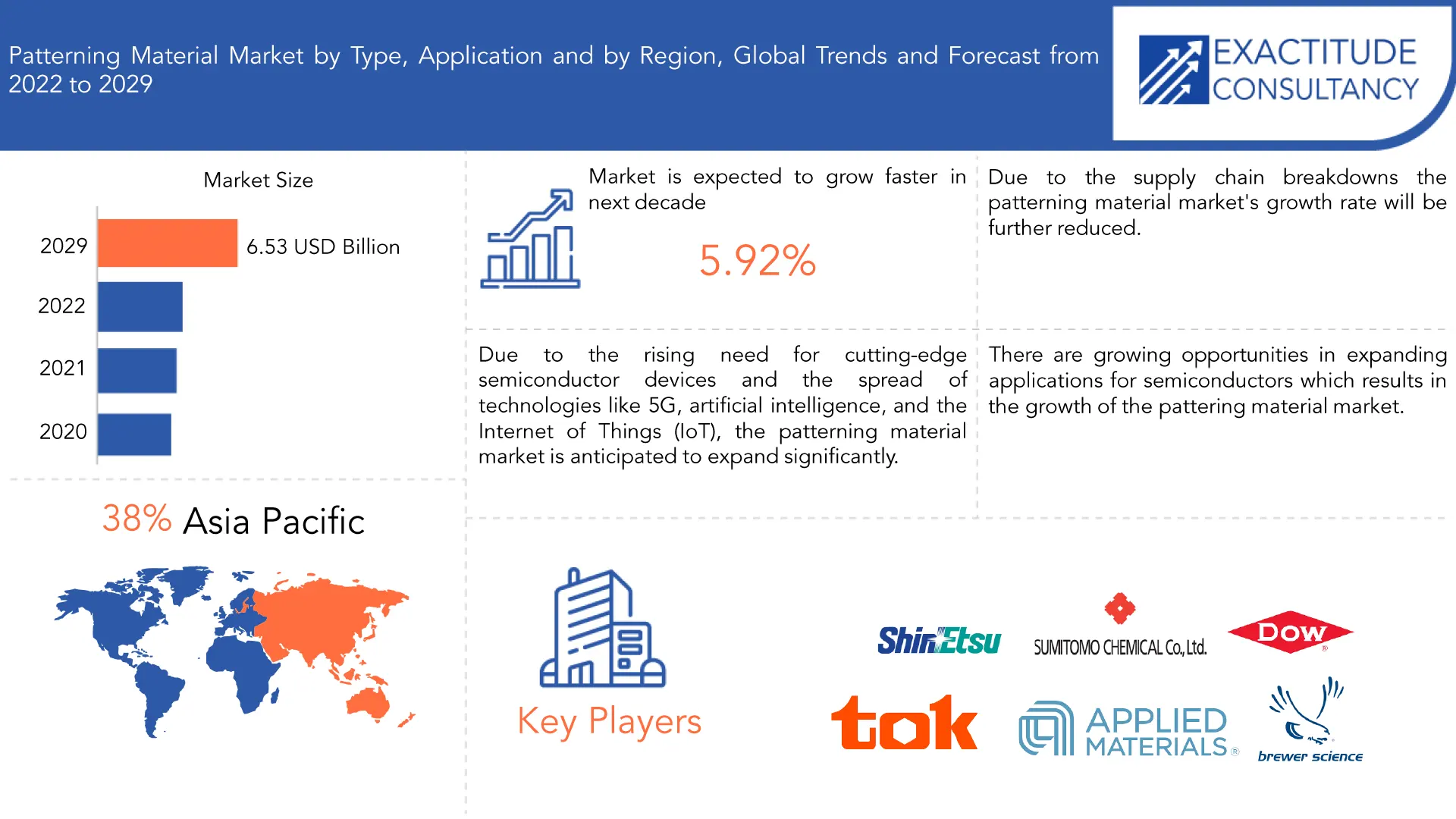
패터닝 소재 시장은 2022년부터 2029년까지 5.92% CAGR로 성장할 것으로 예상됩니다. 2020년에는 약 38억 9천만 달러에 달했습니다. 2029년까지 65억 3천만 달러 이상에 도달할 것으로 예상됩니다.
최첨단 반도체 소자에 대한 수요 증가와 5G, 인공지능 , 사물인터넷 (IoT)과 같은 기술의 확산으로 인해 패터닝 소재 시장이 상당히 확대될 것으로 예상됩니다. 반도체 제조 공정에서 이러한 추세는 정밀하고 고해상도 패터닝 소재에 대한 수요를 증가시킵니다.
반도체 제조 중 패터닝 공정에 사용되는 재료의 개발, 생산 및 유통에 중점을 둔 반도체 산업 분야를 "패터닝 재료 시장"이라고 합니다. 집적 회로(IC) 및 기타 마이크로 전자 부품을 만들기 위해서는 패터닝이 중요한 단계입니다. 여기에는 포토리소그래피 방법을 사용하여 원하는 패턴을 기판에 인쇄하는 것이 포함됩니다. 패터닝 재료는 반도체 웨이퍼에 패턴을 정확하고 정밀하게 전사할 수 있기 때문에 이 기술에 필수적입니다. 포토레지스트, 반사 방지 코팅, 에칭 마스크 및 리소그래피 및 에칭 작업에 사용되는 기타 물질 또는 재료는 이러한 재료의 몇 가지 예입니다. 고해상도 및 고충실도 패턴 전사를 달성하기 위해 특정 광학적, 화학적 및 기계적 특성을 표시하도록 만들어집니다.
[캡션 id="attachment_25653" 정렬="정렬센터" 너비="1920"]
패터닝 소재 시장은 기술이 발전하고 더 작고, 더 강력하고, 더 복잡한 전자 기기에 대한 소비자 수요가 증가함에 따라 더욱 중요해지고 있습니다. 반도체 장치의 축소된 치수와 증가하는 복잡성에 발맞추기 위해 더 나은 분해능, 감도 및 안정성을 갖춘 소재를 개발해야 합니다. 반도체 산업에 최첨단 솔루션을 제공하기 위해 화학 생산자, 장비 공급업체, 소재 개발자를 포함한 다양한 공급업체가 협력하여 패터닝 소재 시장을 형성합니다.
Several dynamic elements that affect the market for patterning materials have an impact on its direction and growth. The demand for better patterning materials is driven by technological developments and advances in the semiconductor sector. Materials with higher resolution, sensitivity, and performance are required as semiconductor devices become more intricate and smaller in size in order to enable perfect pattern transfer. The demand for semiconductor components is fueled by the proliferation of emerging technologies like 5G, artificial intelligence, the Internet of Things (IoT), and autonomous cars. High-performance and high-density integrated circuits are needed for these technologies, which raises the demand for better patterning materials.
The patterning material market is significantly influenced by the geographical distribution of semiconductor manufacturing. Asia Pacific, in particular Taiwan and South Korea, has become one of the primary centres for semiconductor manufacturing. Asia Pacific is a key market for providers due to the concentration of semiconductor manufacturers in these areas, which promotes the demand for patterning materials. In the market for patterning materials, environmental restrictions and sustainability issues are also becoming more and more significant. To reduce the negative effects of the semiconductor manufacturing process on the environment, manufacturers are concentrating on creating eco-friendly materials and procedures.
| ATTRIBUTE | DETAILS |
| Study period | 2020-2029 |
| Base year | 2021 |
| Estimated year | 2022 |
| Forecasted year | 2022-2029 |
| Historical period | 2018-2020 |
| Unit | Value (USD Billion, Thousand Units) |
| Segmentation | By Type, By Application |
| By Type |
|
| By Application |
|
| By Region |
|
Frequently Asked Questions
• What is the worth of patterning material market?
Patterning material market is expected to grow at 5.92% CAGR from 2022 to 2029. it is expected to reach above USD 6.53 billion by 2029
• What is the size of the Asia Pacific in patterning material industry?
Asia Pacific held nearly 38% of patterning material market revenue share in 2021 and will witness expansion in the forecast period.
• What are some of the market's driving forces?
Due to the rising need for cutting-edge semiconductor devices and the spread of technologies like 5G, artificial intelligence, and the Internet of Things (IoT), the patterning material market is anticipated to expand significantly. In semiconductor manufacturing processes, these trends increase the demand for precise and high-resolution patterning materials.
• Which are the top companies to hold the market share in patterning material market?
Microchem Corporation, Shin-Etsu Chemical Co., Ltd., Sumitomo Chemicals Co., Ltd., The Dow Chemical Company, Tokyo Ohka Kogyo Co., Ltd., Applied Materials, Inc., Brewer Science, Inc., DongjinSemichem Co., Ltd., Honeywell Electronic Materials, Inc., JSR Micro, Inc.
• What is the leading segment of patterning material market?
Micro- and nanoscale systems known as MEMS (Micro-Electro-Mechanical Systems) and NEMS (Nano-Electro-Mechanical Systems) integrate mechanical, electrical, and optical components and are used in industries such as consumer electronics, healthcare, and industrial sensing. Glass printed circuit boards are a good choice for high-performance electronic devices as they have benefits including enhanced temperature management and durability. The general demand for patterning materials in the semiconductor market is influenced by these technologies and apparatuses.
Patterning Material Market Segment Analysis
By type the market is segmented into I-line and g-line, positive 248nm, positive 193nm dry resist, positive 193nm immersion resist, others. The older versions of photolithography technologies, I-line and G-line, operate at wavelengths of about 365 nm and 436 nm, respectively. These three distinct photolithography procedures use positive 248 nm, positive 193nm dry resist, and positive 193nm immersion resist as their photoresist materials. Due to their ability to selectively expose and develop the desired patterns on semiconductor substrates, these resist materials are essential for pattern transfer. The total patterning procedure in the semiconductor industry also benefits from the use of additional patterning materials such anti-reflective coatings, etching masks, and speciality chemicals.
By application the market is segmented into DRAM, automotive sensors, MEMS & NEMS devices, glass printed circuit boards, others. Dynamic Random-Access Memory (DRAM) is a type of semiconductor memory that is frequently used to store data in computer systems and other electronic devices. Modern cars rely heavily on automotive sensors to perform a variety of tasks, including driver assistance, safety systems, and engine management. Micro- and nanoscale systems known as MEMS (Micro-Electro-Mechanical Systems) and NEMS (Nano-Electro-Mechanical Systems) integrate mechanical, electrical, and optical components and are used in industries such as consumer electronics, healthcare, and industrial sensing. Glass printed circuit boards are a good choice for high-performance electronic devices as they have benefits including enhanced temperature management and durability. The general demand for patterning materials in the semiconductor market is influenced by these technologies and apparatuses.
[caption id="attachment_25655" align="aligncenter" width="580"]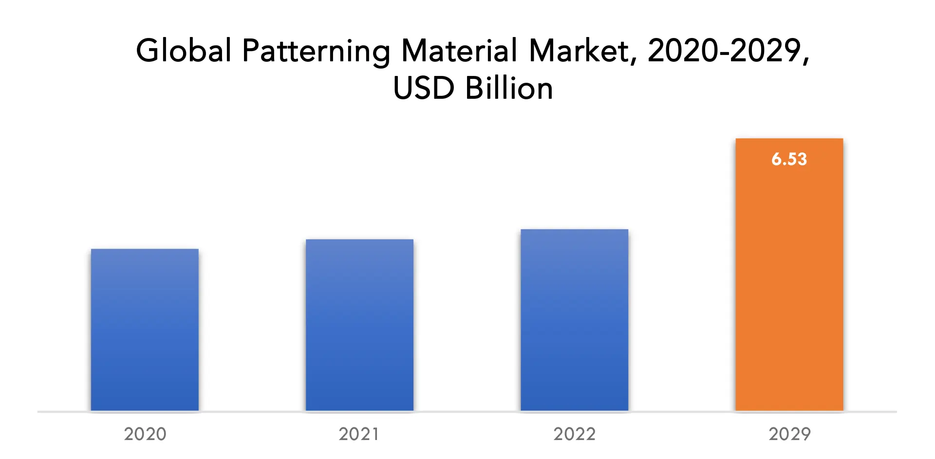
Patterning Material Market Key Players
Patterning material market key players include Microchem Corporation, Shin-Etsu Chemical Co., Ltd., Sumitomo Chemicals Co., Ltd., The Dow Chemical Company, Tokyo Ohka Kogyo Co., Ltd., Applied Materials, Inc., Brewer Science, Inc., DongjinSemichem Co., Ltd., Honeywell Electronic Materials, Inc., JSR Micro, Inc. Recent News:-
March 02, 2023: Shin-Etsu Chemical had developed a silicone rubber for molding that is optimal as an insulation covering material for onboard high-voltage cable in automobiles.
-
May 25, 2023: Dow and New Energy Blue announced collaboration to develop renewable plastic materials from corn residue.
Who Should Buy? Or Key stakeholders
- Semiconductor manufacturers
- Patterning material suppliers
- Equipment manufacturers
- Research institutions
- Design and engineering firms
- Government and regulatory bodies
- Industry associations
- Investors
- Financial institutions
- Trade organizations
- Others
Patterning Material Market Regional Analysis
Patterning material market by region includes North America, Asia-Pacific (APAC), Europe, South America, and Middle East & Africa (MEA).
- North America: includes the US, Canada, Mexico
- Asia Pacific: includes China, Japan, South Korea, India, Australia, ASEAN and Rest of APAC
- Europe: includes UK, Germany, France, Italy, Spain, Russia, and Rest of Europe
- South America: includes Brazil, Argentina and Rest of South America
- Middle East & Africa: includes Turkey, UAE, Saudi Arabia, South Africa, and Rest of MEA
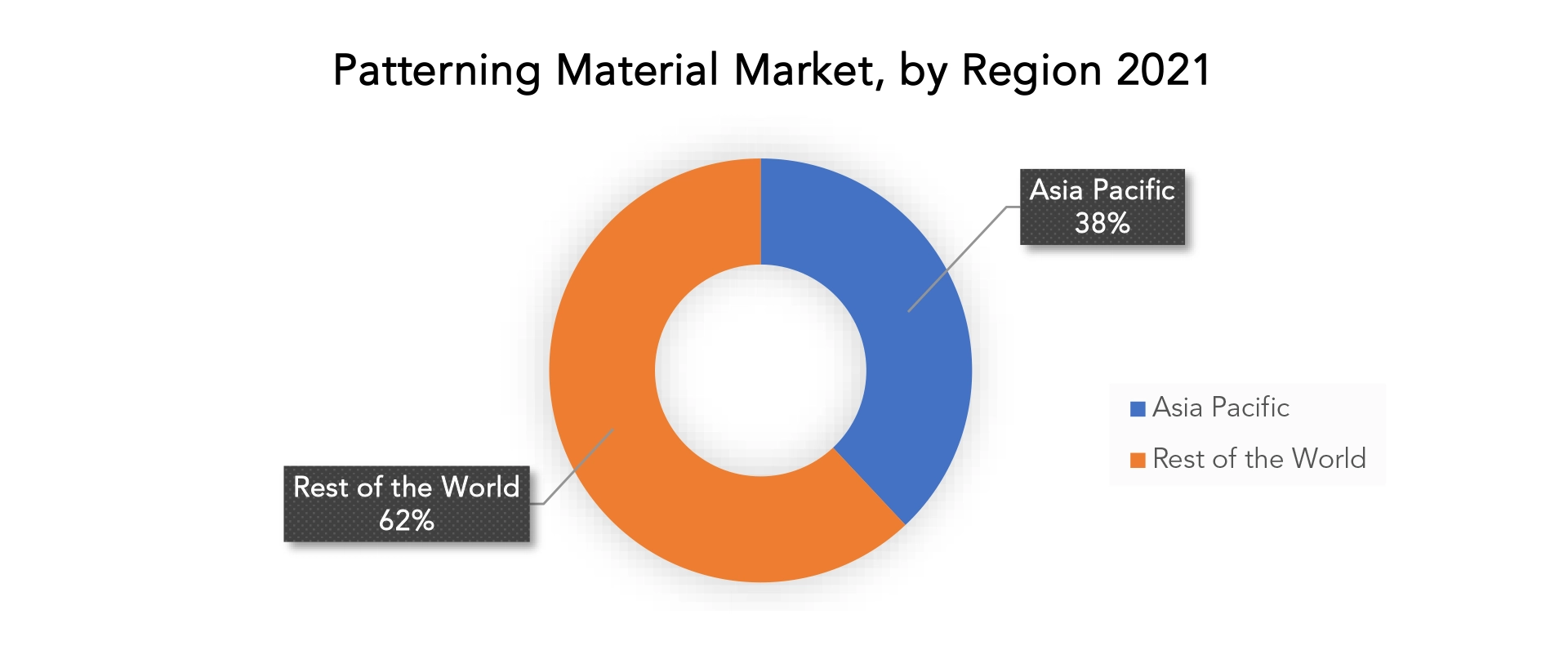
The market for patterning materials in the Asia Pacific region has shown tremendous growth and is predicted to keep growing. The demand for advanced patterning materials is being fueled by elements like the region's significant presence in the semiconductor sector, technical breakthroughs, rising consumer electronics demand, demand for automotive applications, and the emergence of new technologies like 5G and IoT. Additionally, nations like Taiwan, South Korea, China, and Japan have established themselves as significant semiconductor manufacturing hubs, fostering an environment that is favourable for the market for patterning materials to flourish. A strong supply chain, a competent labour base, and the region's emphasis on research and development all help the patterning material market in Asia Pacific thrive.
The market for patterning materials in North America has seen tremendous growth and is expected to continue growing. The market is expanding as a result of elements such the presence of significant semiconductor businesses, technical developments, and rising demand for advanced electronics and communication systems. The demand for cutting-edge patterning materials is fueled by the region's emphasis on research and development, notably in fields like artificial intelligence, driverless vehicles, and high-performance computers. The market for patterning materials in North America is also expanding as a result of the robust ecosystem of research institutions, industry partnerships, and a trained workforce. The region is a vital market for patterning materials due to its focus on innovation and status as a major participant in the global semiconductor industry.
Key Market Segments: Patterning Material Market
Patterning Material Market by Type, 2020-2029, (USD Billion, Thousand Units)- I-Line and G-Line
- Positive 248nm
- Positive 193nm Dry Resist
- Positive 193nm Immersion Resist
- Others
- DRAM
- Automotive Sensors
- MEMS & NEMS Devices
- Glass Printed Circuit Boards
- Others
- North America
- Asia Pacific
- Europe
- South America
- Middle East and Africa
Exactitude Consultancy Services Key Objectives:
- Increasing sales and market share
- Developing new technology
- Improving profitability
- Entering new markets
- Enhancing brand reputation
Key Question Answered
- What is the expected growth rate of the patterning material market over the next 7 years?
- Who are the major players in the patterning material market and what is their market share?
- What are the end-user industries driving demand for market and what is their outlook?
- What are the opportunities for growth in emerging markets such as asia-pacific, middle east, and africa?
- How is the economic environment affecting the patterning material market, including factors such as interest rates, inflation, and exchange rates?
- What is the expected impact of government policies and regulations on the patterning material market?
- What is the current and forecasted size and growth rate of the global patterning material market?
- What are the key drivers of growth in the patterning material market?
- Who are the major players in the market and what is their market share?
- What are the distribution channels and supply chain dynamics in the patterning material market?
- What are the technological advancements and innovations in the patterning material market and their impact on product development and growth?
- What are the regulatory considerations and their impact on the market?
- What are the challenges faced by players in the patterning material market and how are they addressing these challenges?
- What are the opportunities for growth and expansion in the patterning material market?
- What are the product offerings and specifications of leading players in the market?
- What is the pricing trend of patterning material market in the market and what is the impact of raw material prices on the price trend?
- INTRODUCTION
- MARKET DEFINITION
- MARKET SEGMENTATION
- RESEARCH TIMELINES
- ASSUMPTIONS AND LIMITATIONS
- RESEARCH METHODOLOGY
- DATA MINING
- SECONDARY RESEARCH
- PRIMARY RESEARCH
- SUBJECT-MATTER EXPERTS’ ADVICE
- QUALITY CHECKS
- FINAL REVIEW
- DATA TRIANGULATION
- BOTTOM-UP APPROACH
- TOP-DOWN APPROACH
- RESEARCH FLOW
- DATA SOURCES
- DATA MINING
- EXECUTIVE SUMMARY
- MARKET OVERVIEW
- GLOBAL PATTERNING MATERIAL MARKET OUTLOOK
- MARKET DRIVERS
- MARKET RESTRAINTS
- MARKET OPPORTUNITIES
- IMPACT OF COVID-19 ON PATTERNING MATERIAL MARKET
- PORTER’S FIVE FORCES MODEL
- THREAT FROM NEW ENTRANTS
- THREAT FROM SUBSTITUTES
- BARGAINING POWER OF SUPPLIERS
- BARGAINING POWER OF CUSTOMERS
- DEGREE OF COMPETITION
- INDUSTRY VALUE CHAIN ANALYSIS
- GLOBAL PATTERNING MATERIAL MARKET OUTLOOK
- GLOBAL PATTERNING MATERIAL MARKET BY TYPE (USD BILLION, THOUSAND UNITS), 2020-2029
- I-LINE AND G-LINE
- POSITIVE 248NM
- POSITIVE 193NM DRY RESIST
- POSITIVE 193NM IMMERSION RESIST
- OTHERS
- GLOBAL PATTERNING MATERIAL MARKET BY APPLICATION (USD BILLION, THOUSAND UNITS), 2020-2029
- DRAM
- AUTOMOTIVE SENSORS
- MEMS & NEMS DEVICES
- GLASS PRINTED CIRCUIT BOARDS
- OTHERS
- GLOBAL PATTERNING MATERIAL MARKET BY REGION (USD BILLION, THOUSAND UNITS), 2020-2029
- NORTH AMERICA
- US
- CANADA
- MEXICO
- SOUTH AMERICA
- BRAZIL
- ARGENTINA
- COLOMBIA
- REST OF SOUTH AMERICA
- EUROPE
- GERMANY
- UK
- FRANCE
- ITALY
- SPAIN
- RUSSIA
- REST OF EUROPE
- ASIA PACIFIC
- INDIA
- CHINA
- JAPAN
- SOUTH KOREA
- AUSTRALIA
- SOUTH-EAST ASIA
- REST OF ASIA PACIFIC
- MIDDLE EAST AND AFRICA
- UAE
- SAUDI ARABIA
- SOUTH AFRICA
- REST OF MIDDLE EAST AND AFRICA
- NORTH AMERICA
- COMPANY PROFILES*
(BUSINESS OVERVIEW, COMPANY SNAPSHOT, PRODUCTS OFFERED, RECENT DEVELOPMENTS)
- MICROCHEM CORPORATION
- SHIN-ETSU CHEMICAL CO., LTD.
- SUMITOMO CHEMICALS CO., LTD.
- THE DOW CHEMICAL COMPANY
- TOKYO OHKA KOGYO CO., LTD.
- APPLIED MATERIALS, INC.
- BREWER SCIENCE, INC.
- DONGJINSEMICHEM CO., LTD.
- HONEYWELL ELECTRONIC MATERIALS, INC.
- JSR MICRO, INC.
*THE COMPANY LIST IS INDICATIVE
LIST OF TABLES
TABLE 1 GLOBAL PATTERNING MATERIAL MARKET BY TYPE (USD BILLION), 2020-2029
TABLE 2 GLOBAL PATTERNING MATERIAL MARKET BY TYPE (THOUSAND UNITS), 2020-2029
TABLE 3 GLOBAL PATTERNING MATERIAL MARKET BY APPLICATION (USD BILLION), 2020-2029
TABLE 4 GLOBAL PATTERNING MATERIAL MARKET BY APPLICATION (THOUSAND UNITS), 2020-2029
TABLE 5 GLOBAL PATTERNING MATERIAL MARKET BY REGION (USD BILLION), 2020-2029
TABLE 6 GLOBAL PATTERNING MATERIAL MARKET BY REGION (THOUSAND UNITS), 2020-2029
TABLE 7 NORTH AMERICA PATTERNING MATERIAL MARKET BY TYPE (USD BILLION), 2020-2029
TABLE 8 NORTH AMERICA PATTERNING MATERIAL MARKET BY TYPE (THOUSAND UNITS), 2020-2029
TABLE 9 NORTH AMERICA PATTERNING MATERIAL MARKET BY APPLICATION (USD BILLION), 2020-2029
TABLE 10 NORTH AMERICA PATTERNING MATERIAL MARKET BY APPLICATION (THOUSAND UNITS), 2020-2029
TABLE 11 NORTH AMERICA PATTERNING MATERIAL MARKET BY COUNTRY (USD BILLION), 2020-2029
TABLE 12 NORTH AMERICA PATTERNING MATERIAL MARKET BY COUNTRY (THOUSAND UNITS), 2020-2029
TABLE 13 US PATTERNING MATERIAL MARKET BY TYPE (USD BILLION), 2020-2029
TABLE 14 US PATTERNING MATERIAL MARKET BY TYPE (THOUSAND UNITS), 2020-2029
TABLE 15 US PATTERNING MATERIAL MARKET BY APPLICATION (USD BILLION), 2020-2029
TABLE 16 US PATTERNING MATERIAL MARKET BY APPLICATION (THOUSAND UNITS), 2020-2029
TABLE 17 CANADA PATTERNING MATERIAL MARKET BY TYPE (BILLION), 2020-2029
TABLE 18 CANADA PATTERNING MATERIAL MARKET BY TYPE (THOUSAND UNITS), 2020-2029
TABLE 19 CANADA PATTERNING MATERIAL MARKET BY APPLICATION (USD BILLION), 2020-2029
TABLE 20 CANADA PATTERNING MATERIAL MARKET BY APPLICATION (THOUSAND UNITS), 2020-2029
TABLE 21 MEXICO PATTERNING MATERIAL MARKET BY TYPE (USD BILLION), 2020-2029
TABLE 22 MEXICO PATTERNING MATERIAL MARKET BY TYPE (THOUSAND UNITS), 2020-2029
TABLE 23 MEXICO PATTERNING MATERIAL MARKET BY APPLICATION (USD BILLION), 2020-2029
TABLE 24 MEXICO PATTERNING MATERIAL MARKET BY APPLICATION (THOUSAND UNITS), 2020-2029
TABLE 25 SOUTH AMERICA PATTERNING MATERIAL MARKET BY TYPE (USD BILLION), 2020-2029
TABLE 26 SOUTH AMERICA PATTERNING MATERIAL MARKET BY TYPE (THOUSAND UNITS), 2020-2029
TABLE 27 SOUTH AMERICA PATTERNING MATERIAL MARKET BY APPLICATION (USD BILLION), 2020-2029
TABLE 28 SOUTH AMERICA PATTERNING MATERIAL MARKET BY APPLICATION (THOUSAND UNITS), 2020-2029
TABLE 29 SOUTH AMERICA PATTERNING MATERIAL MARKET BY COUNTRY (USD BILLION), 2020-2029
TABLE 30 SOUTH AMERICA PATTERNING MATERIAL MARKET BY COUNTRY (THOUSAND UNITS), 2020-2029
TABLE 31 BRAZIL PATTERNING MATERIAL MARKET BY TYPE (USD BILLION), 2020-2029
TABLE 32 BRAZIL PATTERNING MATERIAL MARKET BY TYPE (THOUSAND UNITS), 2020-2029
TABLE 33 BRAZIL PATTERNING MATERIAL MARKET BY APPLICATION (USD BILLION), 2020-2029
TABLE 34 BRAZIL PATTERNING MATERIAL MARKET BY APPLICATION (THOUSAND UNITS), 2020-2029
TABLE 35 ARGENTINA PATTERNING MATERIAL MARKET BY TYPE (USD BILLION), 2020-2029
TABLE 36 ARGENTINA PATTERNING MATERIAL MARKET BY TYPE (THOUSAND UNITS), 2020-2029
TABLE 37 ARGENTINA PATTERNING MATERIAL MARKET BY APPLICATION (USD BILLION), 2020-2029
TABLE 38 ARGENTINA PATTERNING MATERIAL MARKET BY APPLICATION (THOUSAND UNITS), 2020-2029
TABLE 39 COLOMBIA PATTERNING MATERIAL MARKET BY TYPE (USD BILLION), 2020-2029
TABLE 40 COLOMBIA PATTERNING MATERIAL MARKET BY TYPE (THOUSAND UNITS), 2020-2029
TABLE 41 COLOMBIA PATTERNING MATERIAL MARKET BY APPLICATION (USD BILLION), 2020-2029
TABLE 42 COLOMBIA PATTERNING MATERIAL MARKET BY APPLICATION (THOUSAND UNITS), 2020-2029
TABLE 43 REST OF SOUTH AMERICA PATTERNING MATERIAL MARKET BY TYPE (USD BILLION), 2020-2029
TABLE 44 REST OF SOUTH AMERICA PATTERNING MATERIAL MARKET BY TYPE (THOUSAND UNITS), 2020-2029
TABLE 45 REST OF SOUTH AMERICA PATTERNING MATERIAL MARKET BY APPLICATION (USD BILLION), 2020-2029
TABLE 46 REST OF SOUTH AMERICA PATTERNING MATERIAL MARKET BY APPLICATION (THOUSAND UNITS), 2020-2029
TABLE 47 ASIA-PACIFIC PATTERNING MATERIAL MARKET BY TYPE (USD BILLION), 2020-2029
TABLE 48 ASIA-PACIFIC PATTERNING MATERIAL MARKET BY TYPE (THOUSAND UNITS), 2020-2029
TABLE 49 ASIA-PACIFIC PATTERNING MATERIAL MARKET BY APPLICATION (USD BILLION), 2020-2029
TABLE 50 ASIA-PACIFIC PATTERNING MATERIAL MARKET BY APPLICATION (THOUSAND UNITS), 2020-2029
TABLE 51 ASIA-PACIFIC PATTERNING MATERIAL MARKET BY COUNTRY (USD BILLION), 2020-2029
TABLE 52 ASIA-PACIFIC PATTERNING MATERIAL MARKET BY COUNTRY (THOUSAND UNITS), 2020-2029
TABLE 53 INDIA PATTERNING MATERIAL MARKET BY TYPE (USD BILLION), 2020-2029
TABLE 54 INDIA PATTERNING MATERIAL MARKET BY TYPE (THOUSAND UNITS), 2020-2029
TABLE 55 INDIA PATTERNING MATERIAL MARKET BY APPLICATION (USD BILLION), 2020-2029
TABLE 56 INDIA PATTERNING MATERIAL MARKET BY APPLICATION (THOUSAND UNITS), 2020-2029
TABLE 57 CHINA PATTERNING MATERIAL MARKET BY TYPE (USD BILLION), 2020-2029
TABLE 58 CHINA PATTERNING MATERIAL MARKET BY TYPE (THOUSAND UNITS), 2020-2029
TABLE 59 CHINA PATTERNING MATERIAL MARKET BY APPLICATION (USD BILLION), 2020-2029
TABLE 60 CHINA PATTERNING MATERIAL MARKET BY APPLICATION (THOUSAND UNITS), 2020-2029
TABLE 61 JAPAN PATTERNING MATERIAL MARKET BY TYPE (USD BILLION), 2020-2029
TABLE 62 JAPAN PATTERNING MATERIAL MARKET BY TYPE (THOUSAND UNITS), 2020-2029
TABLE 63 JAPAN PATTERNING MATERIAL MARKET BY APPLICATION (USD BILLION), 2020-2029
TABLE 64 JAPAN PATTERNING MATERIAL MARKET BY APPLICATION (THOUSAND UNITS), 2020-2029
TABLE 65 SOUTH KOREA PATTERNING MATERIAL MARKET BY TYPE (USD BILLION), 2020-2029
TABLE 66 SOUTH KOREA PATTERNING MATERIAL MARKET BY TYPE (THOUSAND UNITS), 2020-2029
TABLE 67 SOUTH KOREA PATTERNING MATERIAL MARKET BY APPLICATION (USD BILLION), 2020-2029
TABLE 68 SOUTH KOREA PATTERNING MATERIAL MARKET BY APPLICATION (THOUSAND UNITS), 2020-2029
TABLE 69 AUSTRALIA PATTERNING MATERIAL MARKET BY TYPE (USD BILLION), 2020-2029
TABLE 70 AUSTRALIA PATTERNING MATERIAL MARKET BY TYPE (THOUSAND UNITS), 2020-2029
TABLE 71 AUSTRALIA PATTERNING MATERIAL MARKET BY APPLICATION (USD BILLION), 2020-2029
TABLE 72 AUSTRALIA PATTERNING MATERIAL MARKET BY APPLICATION (THOUSAND UNITS), 2020-2029
TABLE 73 SOUTH EAST ASIA PATTERNING MATERIAL MARKET BY TYPE (USD BILLION), 2020-2029
TABLE 74 SOUTH EAST ASIA PATTERNING MATERIAL MARKET BY TYPE (THOUSAND UNITS), 2020-2029
TABLE 75 SOUTH EAST ASIA PATTERNING MATERIAL MARKET BY APPLICATION (USD BILLION), 2020-2029
TABLE 76 SOUTH EAST ASIA PATTERNING MATERIAL MARKET BY APPLICATION (THOUSAND UNITS), 2020-2029
TABLE 77 REST OF ASIA PACIFIC PATTERNING MATERIAL MARKET BY TYPE (USD BILLION), 2020-2029
TABLE 78 REST OF ASIA PACIFIC PATTERNING MATERIAL MARKET BY TYPE (THOUSAND UNITS), 2020-2029
TABLE 79 REST OF ASIA PACIFIC PATTERNING MATERIAL MARKET BY APPLICATION (USD BILLION), 2020-2029
TABLE 80 REST OF ASIA PACIFIC PATTERNING MATERIAL MARKET BY APPLICATION (THOUSAND UNITS), 2020-2029
TABLE 81 EUROPE PATTERNING MATERIAL MARKET BY TYPE (USD BILLION), 2020-2029
TABLE 82 EUROPE PATTERNING MATERIAL MARKET BY TYPE (THOUSAND UNITS), 2020-2029
TABLE 83 EUROPE PATTERNING MATERIAL MARKET BY APPLICATION (USD BILLION), 2020-2029
TABLE 84 EUROPE PATTERNING MATERIAL MARKET BY APPLICATION (THOUSAND UNITS), 2020-2029
TABLE 85 EUROPE PATTERNING MATERIAL MARKET BY COUNTRY (USD BILLION), 2020-2029
TABLE 86 EUROPE PATTERNING MATERIAL MARKET BY COUNTRY (THOUSAND UNITS), 2020-2029
TABLE 87 GERMANY PATTERNING MATERIAL MARKET BY TYPE (USD BILLION), 2020-2029
TABLE 88 GERMANY PATTERNING MATERIAL MARKET BY TYPE (THOUSAND UNITS), 2020-2029
TABLE 89 GERMANY PATTERNING MATERIAL MARKET BY APPLICATION (USD BILLION), 2020-2029
TABLE 90 GERMANY PATTERNING MATERIAL MARKET BY APPLICATION (THOUSAND UNITS), 2020-2029
TABLE 91 UK PATTERNING MATERIAL MARKET BY TYPE (USD BILLION), 2020-2029
TABLE 92 UK PATTERNING MATERIAL MARKET BY TYPE (THOUSAND UNITS), 2020-2029
TABLE 93 UK PATTERNING MATERIAL MARKET BY APPLICATION (USD BILLION), 2020-2029
TABLE 94 UK PATTERNING MATERIAL MARKET BY APPLICATION (THOUSAND UNITS), 2020-2029
TABLE 95 FRANCE PATTERNING MATERIAL MARKET BY TYPE (USD BILLION), 2020-2029
TABLE 96 FRANCE PATTERNING MATERIAL MARKET BY TYPE (THOUSAND UNITS), 2020-2029
TABLE 97 FRANCE PATTERNING MATERIAL MARKET BY APPLICATION (USD BILLION), 2020-2029
TABLE 98 FRANCE PATTERNING MATERIAL MARKET BY APPLICATION (THOUSAND UNITS), 2020-2029
TABLE 99 ITALY PATTERNING MATERIAL MARKET BY TYPE (USD BILLION), 2020-2029
TABLE 100 ITALY PATTERNING MATERIAL MARKET BY TYPE (THOUSAND UNITS), 2020-2029
TABLE 101 ITALY PATTERNING MATERIAL MARKET BY APPLICATION (USD BILLION), 2020-2029
TABLE 102 ITALY PATTERNING MATERIAL MARKET BY APPLICATION (THOUSAND UNITS), 2020-2029
TABLE 103 SPAIN PATTERNING MATERIAL MARKET BY TYPE (USD BILLION), 2020-2029
TABLE 104 SPAIN PATTERNING MATERIAL MARKET BY TYPE (THOUSAND UNITS), 2020-2029
TABLE 105 SPAIN PATTERNING MATERIAL MARKET BY APPLICATION (USD BILLION), 2020-2029
TABLE 106 SPAIN PATTERNING MATERIAL MARKET BY APPLICATION (THOUSAND UNITS), 2020-2029
TABLE 107 RUSSIA PATTERNING MATERIAL MARKET BY TYPE (USD BILLION), 2020-2029
TABLE 108 RUSSIA PATTERNING MATERIAL MARKET BY TYPE (THOUSAND UNITS), 2020-2029
TABLE 109 RUSSIA PATTERNING MATERIAL MARKET BY APPLICATION (USD BILLION), 2020-2029
TABLE 110 RUSSIA PATTERNING MATERIAL MARKET BY APPLICATION (THOUSAND UNITS), 2020-2029
TABLE 111 REST OF EUROPE PATTERNING MATERIAL MARKET BY TYPE (USD BILLION), 2020-2029
TABLE 112 REST OF EUROPE PATTERNING MATERIAL MARKET BY TYPE (THOUSAND UNITS), 2020-2029
TABLE 113 REST OF EUROPE PATTERNING MATERIAL MARKET BY APPLICATION (USD BILLION), 2020-2029
TABLE 114 REST OF EUROPE PATTERNING MATERIAL MARKET BY APPLICATION (THOUSAND UNITS), 2020-2029
TABLE 115 MIDDLE EAST AND AFRICA PATTERNING MATERIAL MARKET BY TYPE (USD BILLION), 2020-2029
TABLE 116 MIDDLE EAST AND AFRICA PATTERNING MATERIAL MARKET BY TYPE (THOUSAND UNITS), 2020-2029
TABLE 117 MIDDLE EAST AND AFRICA PATTERNING MATERIAL MARKET BY APPLICATION (USD BILLION), 2020-2029
TABLE 118 MIDDLE EAST AND AFRICA PATTERNING MATERIAL MARKET BY APPLICATION (THOUSAND UNITS), 2020-2029
TABLE 119 MIDDLE EAST AND AFRICA PATTERNING MATERIAL MARKET BY COUNTRY (USD BILLION), 2020-2029
TABLE 120 MIDDLE EAST AND AFRICA PATTERNING MATERIAL MARKET BY COUNTRY (THOUSAND UNITS), 2020-2029
TABLE 121 UAE PATTERNING MATERIAL MARKET BY TYPE (USD BILLION), 2020-2029
TABLE 122 UAE PATTERNING MATERIAL MARKET BY TYPE (THOUSAND UNITS), 2020-2029
TABLE 123 UAE PATTERNING MATERIAL MARKET BY APPLICATION (USD BILLION), 2020-2029
TABLE 124 UAE PATTERNING MATERIAL MARKET BY APPLICATION (THOUSAND UNITS), 2020-2029
TABLE 125 SAUDI ARABIA PATTERNING MATERIAL MARKET BY TYPE (USD BILLION), 2020-2029
TABLE 126 SAUDI ARABIA PATTERNING MATERIAL MARKET BY TYPE (THOUSAND UNITS), 2020-2029
TABLE 127 SAUDI ARABIA PATTERNING MATERIAL MARKET BY APPLICATION (USD BILLION), 2020-2029
TABLE 128 SAUDI ARABIA PATTERNING MATERIAL MARKET BY APPLICATION (THOUSAND UNITS), 2020-2029
TABLE 129 SOUTH AFRICA PATTERNING MATERIAL MARKET BY TYPE (USD BILLION), 2020-2029
TABLE 130 SOUTH AFRICA PATTERNING MATERIAL MARKET BY TYPE (THOUSAND UNITS), 2020-2029
TABLE 131 SOUTH AFRICA PATTERNING MATERIAL MARKET BY APPLICATION (USD BILLION), 2020-2029
TABLE 132 SOUTH AFRICA PATTERNING MATERIAL MARKET BY APPLICATION (THOUSAND UNITS), 2020-2029
TABLE 133 REST OF MIDDLE EAST AND AFRICA PATTERNING MATERIAL MARKET BY TYPE (USD BILLION), 2020-2029
TABLE 134 REST OF MIDDLE EAST AND AFRICA PATTERNING MATERIAL MARKET BY TYPE (THOUSAND UNITS), 2020-2029
TABLE 135 REST OF MIDDLE EAST AND AFRICA PATTERNING MATERIAL MARKET BY APPLICATION (USD BILLION), 2020-2029
TABLE 136 REST OF MIDDLE EAST AND AFRICA PATTERNING MATERIAL MARKET BY APPLICATION (THOUSAND UNITS), 2020-2029
LIST OF FIGURES
FIGURE 1 MARKET DYNAMICS
FIGURE 2 MARKET SEGMENTATION
FIGURE 3 REPORT TIMELINES: YEARS CONSIDERED
FIGURE 4 DATA TRIANGULATION
FIGURE 5 BOTTOM-UP APPROACH
FIGURE 6 TOP-DOWN APPROACH
FIGURE 7 RESEARCH FLOW
FIGURE 8 GLOBAL PATTERNING MATERIAL BY TYPE, USD BILLION, 2020-2029
FIGURE 9 GLOBAL PATTERNING MATERIAL BY APPLICATION, USD BILLION, 2020-2029
FIGURE 10 GLOBAL PATTERNING MATERIAL BY REGION, USD BILLION, 2020-2029
FIGURE 11 PORTER’S FIVE FORCES MODEL
FIGURE 12 GLOBAL PATTERNING MATERIAL BY TYPE, USD BILLION, 2021
FIGURE 13 GLOBAL PATTERNING MATERIAL BY APPLICATION, USD BILLION, 2021
FIGURE 14 GLOBAL PATTERNING MATERIAL BY REGION, USD BILLION, 2021
FIGURE 15 MARKET SHARE ANALYSIS
FIGURE 16 MICROCHEM CORPORATION: COMPANY SNAPSHOT
FIGURE 17 SHIN-ETSU CHEMICAL CO., LTD: COMPANY SNAPSHOT
FIGURE 18 SUMITOMO CHEMICALS CO., LTD: COMPANY SNAPSHOT
FIGURE 19 THE DOW CHEMICAL COMPANY: COMPANY SNAPSHOT
FIGURE 20 TOKYO OHKA KOGYO CO., LTD: COMPANY SNAPSHOT
FIGURE 21 APPLIED MATERIALS, INC: COMPANY SNAPSHOT
FIGURE 22 BREWER SCIENCE, INC: COMPANY SNAPSHOT
FIGURE 23 DONGJINSEMICHEM CO., LTD: COMPANY SNAPSHOT
FIGURE 24 HONEYWELL ELECTRONIC MATERIALS, INC: COMPANY SNAPSHOT
FIGURE 25 JSR MICRO, INC: COMPANY SNAPSHOT
DOWNLOAD FREE SAMPLE REPORT
License Type
SPEAK WITH OUR ANALYST
Want to know more about the report or any specific requirement?
WANT TO CUSTOMIZE THE REPORT?
Our Clients Speak
We asked them to research ‘ Equipment market’ all over the world, and their whole arrangement was helpful to us. thehealthanalytics.com insightful analysis and reports contributed to our current analysis and in creating a future strategy. Besides, the te
Yosuke Mitsui
Senior Associate Construction Equipment Sales & Marketing
We asked them to research ‘Equipment market’ all over the world, and their whole arrangement was helpful to us. thehealthanalytics.com insightful analysis and reports contributed to our current analysis and in creating a future strategy. Besides, the te


